
Samsung and ASML Expand High-NA EUV Push for Next-Gen AI Chips
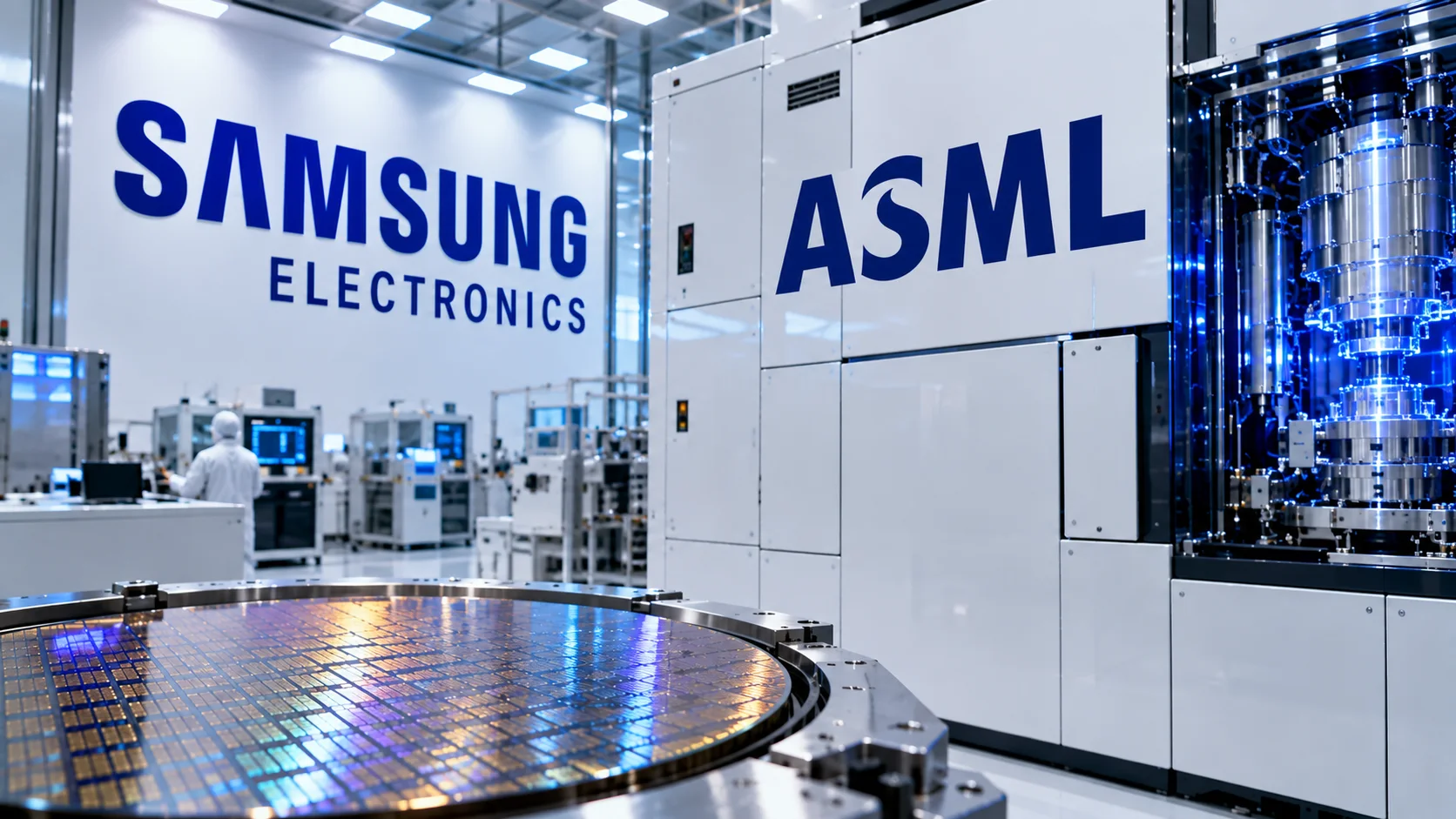
Samsung Electronics and Dutch semiconductor equipment maker ASML are deepening their strategic partnership around High-NA extreme ultraviolet (EUV) lithography as chipmakers prepare for larger and more complex processors used in artificial intelligence and data centres. Samsung will join an industry initiative to develop 12-inch photomasks for High-NA EUV, while ASML is working with major customers on tools capable of manufacturing chips at the upper end of current die sizes.
The collaboration addresses a limitation in the current High-NA EUV ecosystem. ASML’s next-generation systems can print finer chip features than conventional EUV equipment, but their existing smaller masks limit the maximum chip size that can be produced. Larger masks are expected to remove that constraint and make the technology more useful for high-volume manufacturing.
Samsung Plans High-NA EUV for DRAM
Samsung plans to introduce ASML’s High-NA EUV technology into high-volume DRAM manufacturing by 2028, which would make it the first company to use the technology for mass-production DRAM, according to Samsung. The higher numerical aperture gives the EUV system improved resolution, allowing manufacturers to create smaller and more intricate features on semiconductor wafers.
Samsung is also joining the industry effort to develop 12-inch photomask technology. The semiconductor industry has traditionally relied on 6-inch masks, but moving to larger masks could improve fab productivity, reduce manufacturing costs and remove stitching limitations when producing large chips.
ASML Targets Larger AI Chips
ASML is working with major chipmakers including Samsung, Intel and TSMC to adapt High-NA EUV equipment for larger processors such as those designed for AI and data-centre workloads. Existing EUV systems can print chips of roughly 800 square millimetres, a size already used by some large AI processors.
The new larger-mask approach is intended to allow High-NA systems to handle chips of similar scale while retaining their ability to print finer features. ASML plans to demonstrate a pilot line using the larger masks by 2031 and aims to have the technology ready for high-volume manufacturing by 2033.
High-NA EUV Moves Beyond Intel
Intel is currently using ASML’s latest High-NA EUV systems in production, but the technology has not yet reached high-volume manufacturing at Samsung or TSMC. Expanding the usable chip size could make the equipment more attractive to manufacturers that are waiting to deploy the technology at larger production volumes.
TSMC plans to introduce High-NA EUV into advanced-node high-volume manufacturing from 2030. SK Hynix is also evaluating participation in the 12-inch mask initiative and is targeting 2028 for High-NA EUV processes in DRAM mass production.
AI Is Driving the Next Lithography Shift
The push comes as AI processors are becoming larger and more complex. Advanced accelerators need enormous transistor counts and high-speed connectivity to handle workloads such as model training and inference, increasing pressure on manufacturers to improve both chip density and production efficiency.
ASML expects the larger-mask approach could eventually increase the productivity of High-NA systems by around 40%, according to its chief technology officer. For chipmakers, that could help offset the higher cost and complexity associated with adopting next-generation lithography.
Samsung and ASML Strengthen a Critical Partnership
Samsung and ASML have worked together for years on EUV manufacturing, with Samsung using ASML equipment across its advanced memory and foundry operations. Their expanded collaboration now moves toward the supporting infrastructure needed to make High-NA EUV more practical at scale.
The shift to larger masks will require new manufacturing, inspection and handling technologies across the semiconductor supply chain. If the industry meets its planned milestones, High-NA EUV could become an important part of producing future generations of AI processors and advanced memory rather than remaining limited to smaller chips.