
Samsung Reportedly Turns to TSMC’s 3nm Process for Nvidia’s Custom Memory
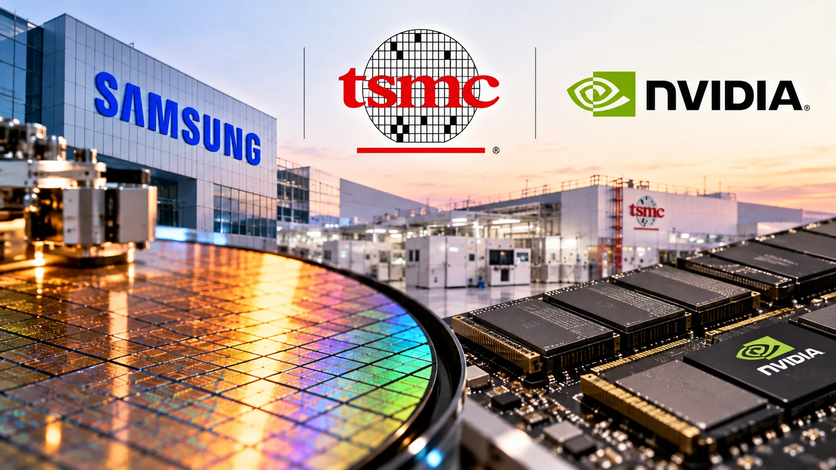
Samsung Electronics is reportedly set to use Taiwan Semiconductor Manufacturing Co.’s (TSMC) 3-nanometre manufacturing process to produce base dies for Nvidia’s next-generation custom high-bandwidth memory, potentially bringing two major semiconductor rivals together at a critical stage of AI chip development.
The reported arrangement concerns Nvidia’s custom memory technology, NVHBM, introduced in August 2026. The design moves Nvidia’s custom memory controller into the high-bandwidth memory (HBM) base die, helping free up space on the processor for computing functions. Nvidia says NVHBM can deliver up to 30% greater memory bandwidth and 15% lower HBM power consumption compared with standard HBM4E.
Nvidia Seeks a Common Manufacturing Approach
The reported plan would see Samsung use TSMC’s 3nm process for the logic base die while continuing to produce the memory dies stacked above it. Seoul Economic Daily reported on October 18 that Nvidia had asked Samsung, SK Hynix and Micron to adopt the same process for NVHBM base dies, alongside a common sixth-generation DRAM technology for the core dies. The report cited industry sources, and the companies have not publicly confirmed those specific manufacturing arrangements.
A common approach could make it easier for Nvidia to validate and integrate memory supplied by different manufacturers. The base die is the logic layer at the bottom of an HBM stack, helping manage communication between the stacked memory dies and the processor. Standardising its manufacturing process could reduce differences between suppliers while supporting Nvidia’s effort to offer custom memory through multiple partners.
A Rare Intersection Between Semiconductor Rivals
Samsung and TSMC compete in contract chip manufacturing, where customers choose foundries to produce processors and other silicon components. Samsung has traditionally pursued an integrated approach to HBM production, manufacturing both memory dies and base dies in-house. Using TSMC’s process for Nvidia’s custom memory would represent a departure from that model for this product, according to the report.
However, the reported arrangement may not rule out Samsung’s own manufacturing options. Seoul Economic Daily also reported that Samsung was examining whether its foundry business could produce the NVHBM base die itself, potentially providing an alternative if TSMC’s available capacity proved insufficient. This remains a reported possibility rather than a confirmed production decision.
Why the Base Die Matters for AI Chips
AI accelerators rely on high-bandwidth memory to move large volumes of data quickly between memory and computing hardware. As AI workloads grow, memory bandwidth, power efficiency and the ability to manufacture advanced components at scale are becoming increasingly important alongside processor performance.
Nvidia’s NVHBM design aims to improve that balance by relocating the memory controller into the HBM stack. If the reported manufacturing plan proceeds, using TSMC’s 3nm process could help Nvidia standardise a key logic component across memory suppliers while drawing on the manufacturing capacity of a company that competes directly with Samsung in foundry services.
For now, Nvidia has publicly described its NVHBM memory architecture, but the specific Samsung–TSMC 3nm production arrangement has not been independently confirmed by the companies.