
IBM’s Anderon Secures $1B U.S. Award to Accelerate Quantum Chip Foundry
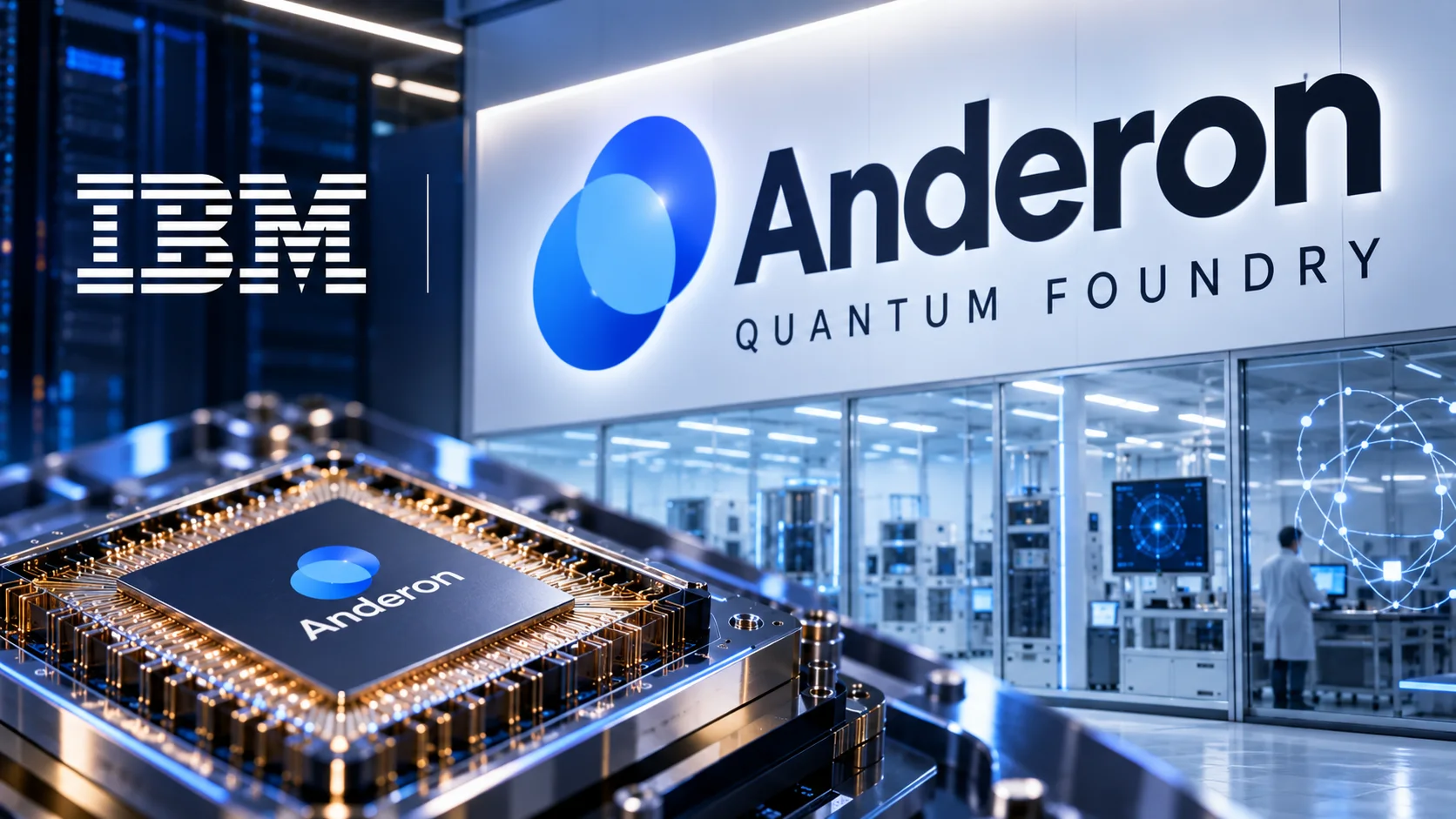
Anderon, an IBM company, has finalized a $1 billion award from the U.S. Department of Commerce under the CHIPS and Science Act to accelerate research and development for a U.S.-based 300mm pure-play quantum wafer foundry. IBM will also provide another $1 billion in cash to support Anderon’s development.
The investment is aimed at building domestic semiconductor manufacturing capabilities for quantum computing and strengthening the U.S. supply chain for advanced quantum technologies.
$1B Award Targets Quantum Wafer Manufacturing
The funding will support Anderon’s work on a 300mm quantum wafer foundry, designed specifically for quantum computing applications. The facility is expected to focus on research, development and manufacturing processes needed to produce quantum devices at scale.
Unlike conventional semiconductor foundries that serve a broad range of chip applications, a pure-play quantum foundry is designed around the specialised requirements of quantum technologies. The project could help establish a dedicated U.S. manufacturing base for quantum hardware.
IBM Adds Another $1B Investment
Alongside the government award, IBM is committing $1 billion in cash to Anderon. The combined investment gives the company significant funding to develop its manufacturing infrastructure and advance quantum-chip research.
The funding also reflects IBM’s broader push to build a complete quantum-computing ecosystem, spanning quantum processors, software, research and manufacturing. A domestic foundry could provide greater control over the production of specialised quantum components.
CHIPS Act Expands Into Quantum Computing
The award comes through the CHIPS and Science Act, the U.S. programme created to strengthen domestic semiconductor manufacturing and reduce reliance on overseas supply chains.
Applying the programme to quantum manufacturing highlights the growing overlap between advanced semiconductor technology and quantum computing. Building specialised fabrication capabilities in the U.S. is becoming increasingly important as companies and governments invest in next-generation computing technologies.
300mm Platform Could Support Future Scale
The planned 300mm wafer platform is designed to provide a manufacturing foundation that can support higher-volume production and more advanced quantum-device development. Moving quantum fabrication toward larger wafer sizes could also help improve manufacturing efficiency and consistency.
Anderon will now use the government and IBM funding to accelerate its R&D programme and establish the infrastructure needed for the foundry. The project adds another major investment to the U.S. effort to develop domestic capabilities in both advanced semiconductors and quantum computing.