
Towa Plans New Japan Factory as AI Chip Demand Drives Advanced Packaging
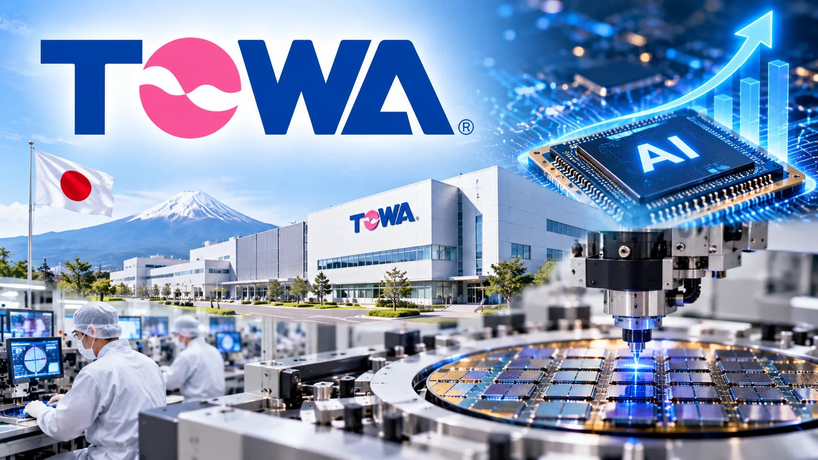
Japanese semiconductor equipment maker Towa plans to build a new factory in Kyoto Prefecture as demand for advanced semiconductor packaging equipment rises alongside the expansion of AI infrastructure.
The company plans to invest about ¥5 billion ($31.6 million) in the facility, with operations targeted for 2029. The plant will produce equipment used in the assembly and packaging processes for advanced semiconductors, including chips designed for AI applications.
The planned factory will add domestic production capacity for Towa, which has relied on overseas facilities and domestic outsourcing for some of its semiconductor equipment manufacturing.
AI Chips Increase Packaging Demand
The expansion comes as AI processors become increasingly complex and require advanced packaging technologies to combine multiple chips and components while maintaining performance and efficiency.
AI accelerators, high-bandwidth memory and other high-performance components are driving investment in advanced packaging as chipmakers look beyond conventional methods to handle increasing computing requirements.
Towa manufactures equipment used in semiconductor assembly and packaging, putting it further down the production chain than companies that fabricate the silicon itself. Its equipment is used to package chips after wafer manufacturing is completed.
Japan Strengthens Domestic Supply Chain
The new facility also reflects Japan's efforts to strengthen its domestic semiconductor supply chain. Building more equipment capacity inside the country could reduce reliance on overseas production and provide local chip manufacturers with a more secure source of manufacturing tools.
Towa's planned investment comes as Japan supports a broader revival of its semiconductor industry, including projects targeting advanced chip production and domestic manufacturing capabilities.
The company expects the Kyoto facility to help meet demand from customers while reinforcing its manufacturing base in Japan.
Advanced Packaging Becomes Strategic
Advanced packaging has become an increasingly important part of the semiconductor industry as chip designers combine processors, memory and other components into increasingly dense systems.
For AI infrastructure, packaging technologies can influence bandwidth, power consumption and the amount of computing that can be delivered within a single system. This has made packaging equipment an increasingly important part of the wider AI semiconductor supply chain.
Towa's new Kyoto plant is therefore aimed not at manufacturing AI chips themselves, but at supplying the equipment needed to assemble and package them. The project gives the company additional capacity as AI-related semiconductor investment continues to expand.